
Verilog module instantiation is a crucial concept in hardware design, enabling the creation and integration of modules within a hierarchical design structure. It allows designers to reuse pre-defined modules, connecting them to build more complex systems. This practice is foundational to efficient digital design, as it promotes modularity, scalability, and reusability.
In this guide, we’ll explore the concept of Verilog module instantiation in detail, starting from its definition and purpose, and progressing to practical examples with code and testbenches. As a beginner, this will help you understand how to connect and utilize modules effectively in your Verilog designs.
What is Module Instantiation in Verilog?
Definition of Module Instantiation
Module instantiation in Verilog refers to the process of creating an instance of a previously defined module within another module. This allows a module to use the functionality of another module, integrating it into a larger design. Each instance is a unique copy of the module, with its own inputs, outputs, and internal state.
Why Module Instantiation is Essential for Hierarchical Design
Hierarchical design is a method of designing complex systems by breaking them into smaller, manageable blocks (modules). Module instantiation plays a vital role in this approach by enabling:
- Reusability: A single module can be instantiated multiple times with different configurations.
- Modularity: Design functionality can be divided into smaller, independent units.
- Ease of Debugging: Isolated modules make it easier to identify and resolve issues.
- Scalability: New functionalities can be added without disrupting existing modules.
Brief Overview of its Role in Connecting Modules
Module instantiation allows modules to communicate by connecting their inputs and outputs. This connection forms the basis of a functional system, where data flows between different parts of the design. For example, a module for an arithmetic logic unit (ALU) can be instantiated within a CPU design to perform arithmetic operations.
Understanding Verilog Modules
Quick Recap of Verilog Modules and Their Structure
Verilog modules are the building blocks of digital designs. A module defines a specific part of a hardware design, such as a logic gate, an arithmetic unit, or a more complex sub-system. Each module can include inputs, outputs, and internal logic, making it reusable and modular.
The structure of a Verilog module typically includes:
- Module Declaration: Specifies the module’s name and ports (inputs, outputs, and sometimes bidirectional signals).
- Port List: Defines the data signals connected to the module.
- Internal Logic: Describes the functionality of the module using assignments, always blocks, or instantiated sub-modules.
- Endmodule: Marks the end of the module definition.
Syntax of a Verilog Module
module module_name (
    input_type input_name1,
    input_type input_name2,
    output_type output_name
);
    // Internal logic
endmodule
Example for a simple AND Gate
module and_gate (
    input a,
    input b,
    output c
);
    assign c = a & b; // Performs AND operation
endmodule
This defines a basic and_gate module that takes two inputs (a and b) and produces an output (c).
Syntax for Module Instantiation
General Syntax for Module Instantiation
In Verilog, module instantiation allows a defined module to be used within another module. This is a key concept in hierarchical design, where complex systems are built by combining smaller, reusable modules.
The general syntax for module instantiation is:
module_name instance_name (
    .port_name(signal_name),
    .port_name(signal_name),
    ...
);
Components of Module Instantiation
module_name- Refers to the name of the module being instantiated.
- It must match the name used in the
moduledefinition. - Example: If the module is defined as
and_gate, themodule_namemust also beand_gate.
instance_name- A unique identifier for the specific instance of the module.
- Used to distinguish between multiple instances of the same module.
- Example:
and1,and2, or any meaningful name likealu_and_gate.
- Port Connections (
.port_name(signal_name))- Maps the module’s ports to the signals in the current module.
.port_name: Refers to the port name in the instantiated module.signal_name: Refers to the signal in the current module that will connect to the port.- This mapping ensures proper communication between modules.
Example: Instantiating an AND Gate Module
AND Gate Module Definition
module and_gate (
    input a,
    input b,
    output c
);
    assign c = a & b;  // Perform AND operation
endmodule
Top-Level Module with Instantiation
module top_module;
    reg x, y;   // Declare input signals
    wire z;     // Declare output signal

    // Instantiate the AND gate module
    and_gate and1 (
        .a(x),
        .b(y),
        .c(z)
    );

    // Test the AND gate functionality
    initial begin
        x = 0; y = 0; #10;
        x = 0; y = 1; #10;
        x = 1; y = 0; #10;
        x = 1; y = 1; #10;
        $finish;
    end

    // Monitor the signals
    initial begin
        $monitor("At time %t: x = %b, y = %b, z = %b", $time, x, y, z);
    end
endmodule
Explanation of Syntax
and_gate: The name of the module being instantiated.and1: The unique instance name for this particular AND gate.- Port Mapping:
.a(x)maps the module’s inputato the signalx..b(y)maps the module’s inputbto the signaly..c(z)maps the module’s outputcto the signalz.
Rules for Module Instantiation
- Unique Instance Names
- Each instance in the same scope must have a unique name.
- Example: If you have multiple AND gates, name them
and1,and2, etc.
- Match Signal Widths
- The width of
signal_namemust match the width of the corresponding port in the module. - Example: If the port is
input [3:0] a, the signalsignal_namemust also be 4 bits wide.
- The width of
- Default Port Order (Optional)
- Ports can also be connected in positional order without explicitly naming them.
Example for port order verilog module instantiation
and_gate and1 (x, y, z); // Positional mappingThis method is less readable and prone to errors; named mapping is recommended.
Instantiating Multiple Instances
In Verilog, you can instantiate the same module multiple times within a design. Each instance operates independently, using its own set of inputs and producing its own outputs. This is useful for designs that require repeated functionality, such as multiple logic gates, adders, or flip-flops.
Syntax for Multiple Instances
module_name instance_name1 (
    .port_name(signal_name1),
    .port_name(signal_name2),
    ...
);

module_name instance_name2 (
    .port_name(signal_name3),
    .port_name(signal_name4),
    ...
);
Here:
module_nameis the name of the module being instantiated.instance_name1,instance_name2, etc., are unique names for each instance..port_name(signal_name)maps the module’s ports to signals in the top-level modul
Example: Instantiating Multiple AND Gate Instances
AND Gate Module Definition
module and_gate (
    input a,
    input b,
    output c
);
    assign c = a & b;  // Perform AND operation
endmodule
Top-Level Module with Multiple Instances
module top_module;
    reg a1, b1, a2, b2; // Inputs for two AND gates
    wire c1, c2;        // Outputs for two AND gates

    // First AND gate instance
    and_gate and1 (
        .a(a1),
        .b(b1),
        .c(c1)
    );

    // Second AND gate instance
    and_gate and2 (
        .a(a2),
        .b(b2),
        .c(c2)
    );

    // Testbench to simulate multiple instances
    initial begin
        // Test first AND gate
        a1 = 0; b1 = 0; #10;
        a1 = 1; b1 = 0; #10;
        a1 = 1; b1 = 1; #10;

        // Test second AND gate
        a2 = 0; b2 = 1; #10;
        a2 = 1; b2 = 0; #10;
        a2 = 1; b2 = 1; #10;

        $finish;
    end

    // Monitor signals for both instances
    initial begin
        $monitor("At time %t: a1 = %b, b1 = %b, c1 = %b | a2 = %b, b2 = %b, c2 = %b",
                 $time, a1, b1, c1, a2, b2, c2);
    end
endmodule
Explanation of Code
- First Instance (
and1):- Input signals:
a1andb1. - Output signal:
c1.
- Input signals:
- Second Instance (
and2):- Input signals:
a2andb2. - Output signal:
c2.
- Input signals:
- Functionality:
- Each AND gate works independently with its respective inputs and outputs.
- The
monitorstatement logs the behavior of both gates during simulation.
Key Takeaways for Multiple Instances
- Unique Instance Names: Each instance must have a unique name (e.g.,
and1,and2). - Independent Inputs and Outputs: Each instance operates independently, based on its connections.
- Scalable Design: Instantiating multiple modules simplifies hierarchical design, making it scalable and modular.
This approach can be extended to larger and more complex systems by instantiating dozens or even hundreds of modules as needed.
Hierarchical Design with Instantiation
Hierarchical design in Verilog involves combining smaller, reusable modules to build more complex systems. This approach is fundamental in digital design, enabling designers to focus on individual components and then integrate them seamlessly into a larger design.
Example: 4-Bit Ripple Carry Adder
A ripple carry adder is a simple design that sums two binary numbers. It uses full adders as building blocks, with each adder handling one bit and passing its carry to the next adder in sequence.
Step 1: Full Adder Module
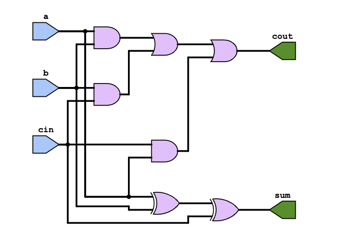
A full adder adds three inputs (two bits and a carry-in) and produces two outputs (sum and carry-out).
module full_adder (
    input a,        // First input bit
    input b,        // Second input bit
    input cin,      // Carry-in
    output sum,     // Sum output
    output cout     // Carry-out
);
    assign sum = a ^ b ^ cin;    // XOR for sum
    assign cout = (a & b) | (b & cin) | (cin & a);  // OR of ANDs for carry-out
endmodule
Here is the schematic of the above design code
Step 2: 4-Bit Ripple Carry Adder Module
The ripple carry adder instantiates four full adders to add two 4-bit numbers.
module ripple_carry_adder_4bit (
    input [3:0] a,  // 4-bit input A
    input [3:0] b,  // 4-bit input B
    input cin,      // Initial carry-in
    output [3:0] sum, // 4-bit sum output
    output cout      // Final carry-out
);
    wire c1, c2, c3; // Intermediate carry signals

    // Instantiate four full adders
    full_adder fa0 (.a(a[0]), .b(b[0]), .cin(cin), .sum(sum[0]), .cout(c1));
    full_adder fa1 (.a(a[1]), .b(b[1]), .cin(c1), .sum(sum[1]), .cout(c2));
    full_adder fa2 (.a(a[2]), .b(b[2]), .cin(c2), .sum(sum[2]), .cout(c3));
    full_adder fa3 (.a(a[3]), .b(b[3]), .cin(c3), .sum(sum[3]), .cout(cout));
endmodule
Step 3: Testbench for the 4-Bit Ripple Carry Adder
The testbench applies various input combinations to verify the functionality of the ripple carry adder.
module testbench;
    reg [3:0] a, b;   // 4-bit inputs
    reg cin;          // Carry-in
    wire [3:0] sum;   // Sum output
    wire cout;        // Carry-out

    // Instantiate the 4-bit ripple carry adder
    ripple_carry_adder_4bit rca (
        .a(a),
        .b(b),
        .cin(cin),
        .sum(sum),
        .cout(cout)
    );

    // Apply test vectors
    initial begin
        $monitor("At time %t: a = %b, b = %b, cin = %b, sum = %b, cout = %b",
                 $time, a, b, cin, sum, cout);

        // Test case 1
        a = 4'b0001; b = 4'b0010; cin = 0; #10;
        // Test case 2
        a = 4'b0110; b = 4'b0101; cin = 1; #10;
        // Test case 3
        a = 4'b1111; b = 4'b1111; cin = 0; #10;
        // Test case 4
        a = 4'b1001; b = 4'b0110; cin = 1; #10;

        $finish;
    end
endmodule
Explanation of Hierarchical Design
- Full Adder as a Building Block
- The full adder performs the basic addition operation for a single bit.
- 4-Bit Ripple Carry Adder
- Instantiates four full adders, chaining their carry-out to the carry-in of the next adder.
- Testbench
- Verifies the entire hierarchical design by applying various input combinations and monitoring the outputs.
Key Takeaways
- Reuse and Modularity: By reusing the
full_addermodule, the ripple carry adder demonstrates the power of hierarchical design. - Scalability: Designs can easily scale by adding more instances (e.g., an 8-bit adder).
- Clear Structure: Hierarchical design makes debugging and extending systems easier.
This approach can be expanded for larger systems, such as multipliers, ALUs, or even processors, using similar principles.
Common Mistakes and Debugging Tips
When working with module instantiation in Verilog, mistakes can occur due to incorrect port connections, naming conflicts, or signal mismatches. Debugging these issues is a crucial skill for beginners. Let’s explore common mistakes and provide actionable debugging tips to resolve them.
Incorrect Port Mapping
One of the most frequent errors in module instantiation is incorrect mapping of ports to signals. This can lead to unexpected behavior or simulation failures.
Example of Incorrect Port Mapping:
module my_module (
    input a,
    input b,
    output c
);

// Intended to connect `a` to `x` and `b` to `y`
// But mistakenly swapped `x` and `y`
my_module instance1 (
    .a(y),
    .b(x),
    .c(z)
);
Debugging Tip:
- Double-check the module’s port declarations and ensure the signals are mapped to the correct ports.
- Use descriptive signal names to minimize confusion (e.g.,
input_ainstead ofa).
Corrected Code:
my_module instance1 (
    .a(x),
    .b(y),
    .c(z)
);
2. Naming Conflicts
Using duplicate names for different instances or signals can cause issues in hierarchical designs.
Example of Naming Conflict:
module my_module (
    input a,
    input b,
    output c
);
endmodule

module top;
    wire a, b, c; // Signal names conflict with module inputs
    my_module my_module (.a(a), .b(b), .c(c)); // Confusion arises here
endmodule
Debugging Tip:
- Ensure signal names in the top-level module do not conflict with the internal port names of instantiated modules.
- Use a consistent naming convention, such as appending
_topfor top-level signals.
Corrected Code:
module top;
    wire a_top, b_top, c_top; // Unique signal names
    my_module instance1 (.a(a_top), .b(b_top), .c(c_top));
endmodule
3. Signals Not Connected Properly to Ports
Leaving ports unconnected or improperly connected can cause logic errors.
Example of Unconnected Signal:
module my_module (
    input a,
    input b,
    output c
);
endmodule

module top;
    wire a, c;
    my_module instance1 (.a(a), .b(), .c(c)); // Port `b` is unconnected
endmodule
Debugging Tip:
- Use tools like simulation warnings or linting tools to identify unconnected ports.
- If a port is intentionally left unconnected, use a placeholder signal (
openor1'b0) for clarity.
Corrected Code:
module top;
    wire a, b, c;
    my_module instance1 (.a(a), .b(b), .c(c)); // Ensure all ports are connected
endmodule
Mismatched Port Sizes
Mismatching the bit widths of ports and connected signals can lead to unexpected results.
Example of Mismatched Port Sizes:
module my_module (
    input [3:0] a,
    output [3:0] b
);
endmodule

module top;
    wire [1:0] a; // Only 2 bits
    wire [3:0] b;
    my_module instance1 (.a(a), .b(b)); // Width mismatch
endmodule
Debugging Tip:
- Ensure that the connected signals match the width of the module ports.
- Use explicit signal slicing or extension to resolve mismatches.
Corrected Code:
module top;
    wire [3:0] a;
    wire [3:0] b;
    my_module instance1 (.a(a), .b(b));
endmodule
General Debugging Tips for Module Instantiation
- Use Simulation Tools:
- Use simulators like ModelSim, Xilinx Vivado, or Synopsys VCS to identify issues.
- Check waveform outputs for unexpected behavior.
- Employ Assertions:
- Use assertions to validate the behavior of instantiated modules during simulation.
- Modular Testing:
- Test individual modules separately before integrating them into a larger design.
- Read Warning and Error Messages:
- Carefully review compilation and simulation logs for clues about instantiation errors.
- Document Connections:
- Maintain clear documentation of port-to-signal mappings, especially for complex designs.
Module instantiation is a cornerstone of hierarchical design in Verilog. It enables the creation of complex digital systems by integrating smaller, reusable blocks. Through proper instantiation, you can build scalable, efficient, and maintainable designs.
Key Takeaways:
- Clear Naming: Use descriptive names for signals and instances to improve code clarity.
- Named Port Mapping: Always prefer named port mapping for better readability, especially in large designs.
- Modular Testing: Test individual modules rigorously before combining them.
- Documentation: Provide clear documentation for your design to aid collaboration and maintenance.
- Scalability: Utilize parameters for flexible and scalable module designs.
By following these practices, you can minimize errors, enhance the quality of your designs, and lay a solid foundation for more advanced Verilog concepts. Now that you understand the fundamentals of module instantiation, try experimenting with your designs to see these principles in action!
I’m an electrical engineer and chip designer pursuing a Master’s in Electrical Engineering at The University of Texas at Dallas. Passionate about digital design, I created Logic Flick to simplify complex concepts in Verilog, SystemVerilog, and UVM. Join me on this electrifying journey as we explore the world of digital electronics together!