
Verilog is a widely-used hardware description language (HDL) essential for designing and simulating digital circuits. It allows engineers to describe circuit behavior, structure, and timing, making it an indispensable tool in hardware design. Learning Verilog can seem daunting at first, but working through Verilog examples simplifies the process by bridging theoretical concepts with practical implementation.
Beginners often benefit from hands-on experience, and Verilog examples provide an excellent foundation. By exploring basic circuits like logic gates, flip-flops, and multiplexers, learners can understand Verilog syntax and its applications in digital design. These examples also demonstrate how Verilog captures the intricacies of both combinational and sequential circuits, empowering designers to translate ideas into hardware efficiently.
This guide presents simple yet powerful Verilog examples to help you kickstart your journey in hardware design. With a focus on clarity and step-by-step explanation, these examples are crafted to ensure a smooth introduction to Verilog. Whether you’re a student, an aspiring engineer, or a hobbyist, diving into these examples will enhance your understanding of digital circuit design and Verilog coding.
Why Learn Verilog Through Examples?
Verilog’s syntax and features may initially appear abstract, but learning through examples bridges the gap between theoretical concepts and practical implementation. Each example demonstrates key concepts in context, enabling a hands-on understanding of the language.
By exploring Verilog examples, you can:
- Develop a practical understanding of how to write Verilog code.
- Learn to debug and simulate designs effectively.
- Gain confidence in applying Verilog to real-world digital design challenges.
These examples act as building blocks, enabling learners to progress from simple combinational logic to complex sequential systems.
Example 1: Basic AND Gate
module AND_Gate(
    input A,
    input B,
    output Y
);
    assign Y = A & B; // Logical AND operation
endmodule
Explanation
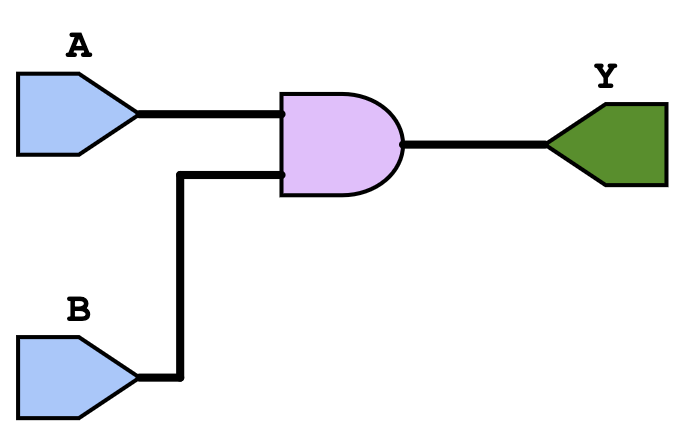
module: Defines a design block in Verilog. Here, the module is namedAND_Gate.inputandoutput: Specify the inputs (AandB) and the output (Y) of the AND gate.assign: Performs the logical AND operation (A & B) and assigns the result toY.
Schematic of the Above verilog
Simulation Steps
- Write a testbench to provide inputs and observe the output.
- Simulate the design using an EDA tool like ModelSim or Xilinx Vivado.
Below is the test bench code for the above design
module Test_AND_Gate;
    reg A, B;          // Declare test inputs
    wire Y;            // Declare the output wire

    AND_Gate uut (     // Instantiate the AND_Gate module
        .A(A),
        .B(B),
        .Y(Y)
    );

    initial begin
        // Apply test cases
        A = 0; B = 0; #10;
        A = 0; B = 1; #10;
        A = 1; B = 0; #10;
        A = 1; B = 1; #10;

        $finish;       // End simulation
    end
endmodule
Here is the output waveform of and gate

Expected Output
The output Y will reflect the logical AND operation:
A = 0, B = 0 → Y = 0A = 0, B = 1 → Y = 0A = 1, B = 0 → Y = 0A = 1, B = 1 → Y = 1
Example 2: Half Adder
module Half_Adder(
    input A,
    input B,
    output Sum,
    output Carry
);
    assign Sum = A ^ B;    // XOR for Sum
    assign Carry = A & B;  // AND for Carry
endmodule
Explanation
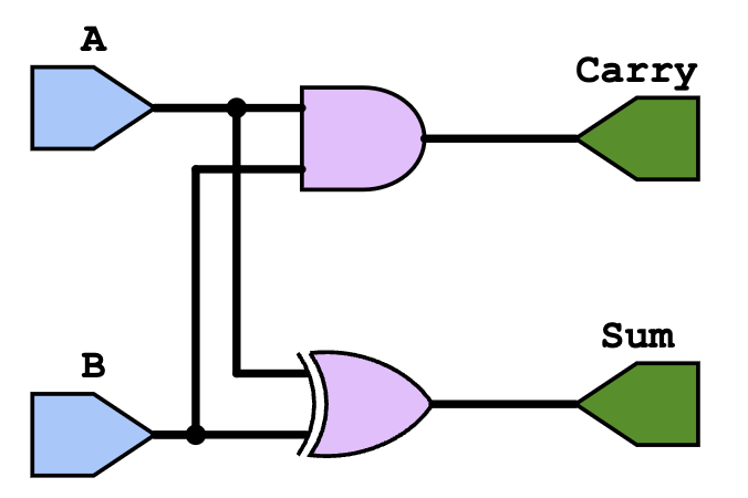
- The
Half_Addermodule implements a simple combinational circuit to add two binary digits. Sumis computed using the XOR operation (A ^ B).Carryis generated using the AND operation (A & B).
Here is the schematic of the above code
Simulation Steps
- Create a testbench to apply various combinations of
AandB. - Observe the values of
SumandCarryto verify correctness.
Below is the test bench code for the above design
module Test_Half_Adder;
    reg A, B;               // Declare inputs
    wire Sum, Carry;        // Declare outputs

    Half_Adder uut (        // Instantiate the Half_Adder module
        .A(A),
        .B(B),
        .Sum(Sum),
        .Carry(Carry)
    );

    initial begin
        // Apply test cases
        A = 0; B = 0; #10;
        A = 0; B = 1; #10;
        A = 1; B = 0; #10;
        A = 1; B = 1; #10;

        $finish;            // End simulation
    end
endmodule
Expected Output
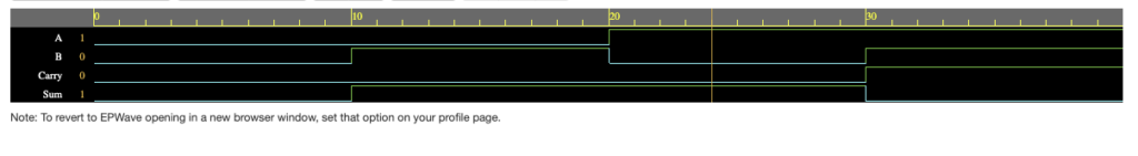
The half adder will generate:
A = 0, B = 0 → Sum = 0, Carry = 0A = 0, B = 1 → Sum = 1, Carry = 0A = 1, B = 0 → Sum = 1, Carry = 0A = 1, B = 1 → Sum = 0, Carry = 1
Simulation output of Half adder
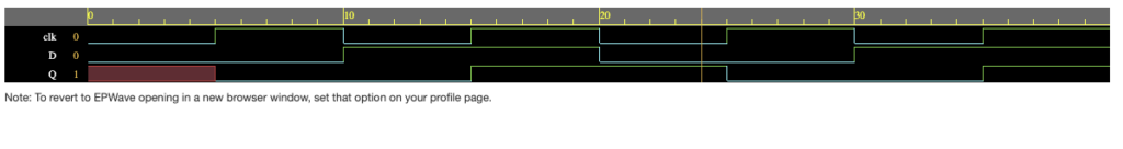
Example 3: Flip-Flop (Sequential Circuit)
Flip-flops are fundamental building blocks in sequential circuits, storing data based on clock inputs. The D (data) flip-flop is one of the simplest types of flip-flops. It stores the input value (D) on the rising edge of the clock and retains the value until the next edge.
Here is the verilog code for a simple D flip flip:
module D_FlipFlop (
    input D,            // Data input
    input clk,          // Clock input
    output reg Q        // Data output (register type)
);
    always @(posedge clk) begin
        Q <= D;         // Store the value of D on clock's rising edge
    end
endmodule
Explanation
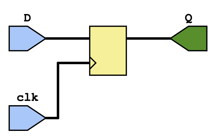
always @(posedge clk): This statement triggers the block whenever the clock signal transitions from low to high (rising edge).- Sequential Logic: Unlike combinational circuits, sequential circuits like flip-flops depend on the clock.
reg: The outputQis declared as aregbecause it holds its value across clock cycles.
Schematic of the above code
Simulation Steps
- Write a testbench to provide inputs (
Dandclk) and observe the behavior ofQ. - Simulate the design using an HDL simulator.
Here is the Test Bench for the above code
module Test_D_FlipFlop;
    reg D, clk;        // Test inputs
    wire Q;            // Test output

    D_FlipFlop uut (   // Instantiate the D_FlipFlop module
        .D(D),
        .clk(clk),
        .Q(Q)
    );

    initial begin
        // Clock generation
        clk = 0;
        forever #5 clk = ~clk; // Toggle clock every 5 time units
    end

    initial begin
        // Apply test cases
        D = 0; #10;
        D = 1; #10;
        D = 0; #10;
        D = 1; #10;

        $finish; // End simulation
    end
endmodule
Expected Output
The flip-flop output Q follows the input D at every rising edge of the clock:
- When
D = 0and clock rises,Q = 0. - When
D = 1and clock rises,Q = 1.
Here is the output waveform
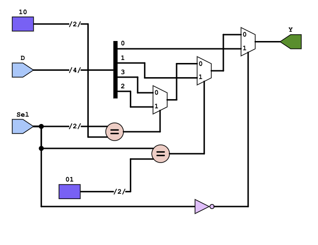
Example 4: Multiplexer (MUX)
A multiplexer is a combinational circuit that selects one of many inputs based on a select signal. A 4:1 multiplexer, for example, has four data inputs, two select lines, and one output. Mind that I have considered the all the 4 bits of input D as different inputs. Hence a 4 to 1 mux.
module MUX_4to1 (
    input [3:0] D,      // 4 data inputs
    input [1:0] Sel,    // 2-bit select input
    output Y            // Output
);
    assign Y = (Sel == 2'b00) ? D[0] :
               (Sel == 2'b01) ? D[1] :
               (Sel == 2'b10) ? D[2] :
               D[3];          // Default case
endmodule
Explanation
input [3:0] D: Represents four data inputs (D[0]toD[3]).input [1:0] Sel: Selects one of the four inputs.- Conditional Logic: The
assignstatement implements a series of conditional checks to determine which input is routed to the output (Y).
Here is the schematic of the above design code
Simulation Steps
- Create a testbench to apply different combinations of data inputs and select signals.
- Observe the output for correctness.
module Test_MUX_4to1;
    reg [3:0] D;        // Test data inputs
    reg [1:0] Sel;      // Test select signal
    wire Y;             // Test output

    MUX_4to1 uut (      // Instantiate the MUX_4to1 module
        .D(D),
        .Sel(Sel),
        .Y(Y)
    );

    initial begin
        // Apply test cases
        D = 4'b1010; Sel = 2'b00; #10; // Output should be D[0] = 1
        D = 4'b1010; Sel = 2'b01; #10; // Output should be D[1] = 0
        D = 4'b1010; Sel = 2'b10; #10; // Output should be D[2] = 1
        D = 4'b1010; Sel = 2'b11; #10; // Output should be D[3] = 0

        $finish; // End simulation
    end
endmodule
Expected Output
The output Y corresponds to the selected input:
Sel = 00 → Y = D[0].Sel = 01 → Y = D[1].Sel = 10 → Y = D[2].Sel = 11 → Y = D[3].
Here is the simulation output

Best Practices for Beginners
Structuring Verilog Code for Readability
- Use Comments: Clearly annotate your code to explain functionality.
- Follow Consistent Naming Conventions: Use meaningful names for modules, signals, and variables.
- Modular Design: Break large designs into smaller, reusable modules.
Importance of Modular Design and Reusability
Modularity ensures that designs are easy to understand, debug, and extend. For example, a half adder module can be reused in a full adder, and a multiplexer module can be a building block for larger systems.
Debugging Tips and Tools for Testing Verilog Designs
- Use Assertions: Assertions can verify that certain conditions hold during simulation.
- Simulate Extensively: Test modules with diverse edge cases.
- Waveform Analysis: Use simulation tools to view signal transitions and debug issues.
- Start Simple: Begin with simple designs and test thoroughly before integrating them into larger systems.
By adhering to these best practices, beginners can develop robust and maintainable Verilog designs while mastering the foundational concepts of hardware description
I’m an electrical engineer and chip designer pursuing a Master’s in Electrical Engineering at The University of Texas at Dallas. Passionate about digital design, I created Logic Flick to simplify complex concepts in Verilog, SystemVerilog, and UVM. Join me on this electrifying journey as we explore the world of digital electronics together!