
In the world of electronics, the ASIC design flow is a fundamental process that transforms innovative ideas into cutting-edge, application-specific integrated circuits. These circuits are tailored to meet the unique needs of specialized applications, making them an indispensable part of modern technology. This blog dives deep into the ASIC design flow, its importance, and how Verilog plays a pivotal role in ensuring successful chip design and fabrication.
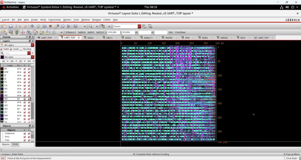
This is a UART chip designed by me and my friend Sumukh, successfully completed up to the Place and Route (PnR) stage.
Introduction
Overview of ASIC Design
Application-Specific Integrated Circuits (ASICs) are custom-designed chips created to perform specific tasks. Unlike general-purpose chips, such as microprocessors, ASICs are optimized for efficiency, speed, and performance within their target applications. Industries like telecommunications, automotive, and consumer electronics heavily rely on ASICs for their specialized requirements.
Importance of Verilog in the ASIC Design Flow
Verilog, a widely used hardware description language (HDL), is integral to the ASIC design flow. It allows engineers to model, simulate, and verify digital circuits at various stages of the design process. From behavioral modeling to synthesis and verification, Verilog ensures precision and efficiency in developing complex hardware architectures.
Scope and Objectives of This Blog
This blog aims to provide a comprehensive understanding of the ASIC design flow, emphasizing Verilog’s role in each stage. Whether you’re a budding engineer or an industry professional, this guide will enhance your grasp of ASIC design and its practical implementation.
What is an ASIC?
Definition and Examples of ASICs
An Application-Specific Integrated Circuit (ASIC) is a custom-designed semiconductor chip created for a specific purpose. Unlike programmable chips like FPGAs, ASICs are hardwired to perform predefined functions. Examples of ASICs include:
- Graphics Processing Units (GPUs) optimized for rendering graphics.
- Cryptographic chips used in secure communication.
- AI accelerators for machine learning tasks.
Key Differences Between ASICs and FPGAs
While ASICs and FPGAs (Field-Programmable Gate Arrays) are both used in hardware design, their differences lie in flexibility and application:
- ASICs are fixed-function chips designed for specific tasks, offering high efficiency and performance.
- FPGAs are programmable and versatile, allowing reconfiguration for different applications but often consuming more power and resources.
Why ASICs Are Crucial
ASICs are critical for applications requiring optimized performance, lower power consumption, and reduced size. In industries like automotive (e.g., advanced driver-assistance systems) and telecommunications (e.g., 5G base stations), ASICs provide the specialized hardware needed to meet stringent requirements.
Overview of the ASIC Design Flow
The ASIC design flow is a structured sequence of stages that engineers follow to design, verify, and fabricate application-specific integrated circuits. Each step is crucial for ensuring that the final chip meets design specifications and performs reliably.
High-Level Stages in the ASIC Design Flow
- Specification
- Define the functionality, performance, power, and area requirements of the ASIC.
- Collaborate with stakeholders to establish clear design goals.
- Design and Modeling
- Use Verilog to create behavioral and structural models of the circuit.
- Simulate the models to verify functionality against the specifications.
- Verification
- Perform functional and formal verification to ensure the design operates as intended.
- Use testbenches written in Verilog to identify and eliminate potential bugs.
- Synthesis
- Translate the Verilog design into a gate-level netlist using synthesis tools.
- Optimize the netlist for area, power, and performance constraints.
- Physical Design
- Convert the gate-level netlist into a physical layout, placing and routing the components.
- Ensure the layout adheres to manufacturing design rules and constraints.
- Fabrication and Testing
- Manufacture the ASIC using semiconductor fabrication processes.
- Test the fabricated chip to verify functionality and performance.
Role of Verilog in the ASIC Design Flow
Specification
While Verilog doesn’t directly contribute to the specification phase, its syntax and modeling capabilities guide how design requirements are translated into code. Engineers use Verilog to create templates and high-level representations of the desired functionality.
Design and Modeling
Verilog is the backbone of the modeling phase. Engineers use Verilog to describe the circuit at multiple levels:
- Behavioral Level: Define how the circuit should behave without specifying implementation details.
- RTL (Register Transfer Level): Focus on data flow between registers and logic operations.
- Gate Level: Represent the design in terms of logic gates and their connections.
Verification
Verilog is instrumental in creating testbenches, which simulate the circuit’s behavior under different conditions. These testbenches validate that the design meets its functional requirements. Tools like ModelSim and Synopsys VCS use Verilog to execute simulation tasks efficiently.
Synthesis
In the synthesis stage, Verilog code is transformed into a gate-level netlist. Tools like Synopsys Design Compiler process Verilog descriptions to generate optimized hardware that adheres to the specified constraints.
Physical Design
Although physical design relies more on Electronic Design Automation (EDA) tools, the gate-level netlist generated from Verilog synthesis serves as the foundation for this stage. Verilog’s clarity and accuracy ensure that the netlist accurately represents the intended design.
Fabrication and Testing
During testing, Verilog testbenches are reused to verify that the fabricated chip functions correctly. Post-silicon validation leverages Verilog-based simulation models to confirm performance and identify potential defects.
Why Mastering the ASIC Design Flow is Important
For engineers in the semiconductor industry, understanding the ASIC design flow is essential. It provides a structured framework for tackling complex hardware design challenges. Proficiency in Verilog further enhances one’s ability to model, simulate, and verify designs effectively.
Detailed Stages of ASIC Design Flow
Specification
The specification phase is the starting point of the ASIC design flow. It defines the chip’s intended functionality, performance metrics, power consumption limits, and design constraints. These specifications are created based on application requirements and stakeholder input, forming the blueprint for the design.
Design Entry and RTL Coding
In this stage, the chip’s functionality is described using Register Transfer Level (RTL) coding. Verilog is the preferred language due to its efficiency in hardware description.
- Modular Design: The circuit is divided into smaller, reusable modules for better organization and maintainability.
- Code Organization: Structuring code for clarity ensures ease of debugging and verification.
Engineers simulate individual modules and integrate them into the complete design, maintaining consistency with the specifications.
Functional Verification
Functional verification ensures that the design behaves as expected before proceeding to synthesis. This phase involves:
- Simulation: Verilog-based testbenches are written to validate the functionality under various scenarios.
- Debugging: Identifying and resolving logical and functional issues early in the process.
Verification tools like ModelSim and Synopsys VCS are commonly used for high-fidelity simulations.
Synthesis
Synthesis converts the Verilog RTL code into a gate-level netlist, which is a detailed representation of logic gates and their interconnections. Key activities in this phase include:
- Optimization: Ensuring the design meets constraints like area, power, and timing.
- Tools: EDA tools such as Synopsys Design Compiler are employed for synthesis tasks.
The generated netlist forms the basis for the subsequent physical design phase.
Physical Design
This stage translates the gate-level netlist into a physical layout that can be fabricated. It includes:
- Place and Route (P&R): Arranging standard cells and routing interconnections based on the netlist.
- Timing Analysis: Ensuring signal timing meets constraints to prevent errors like hold or setup violations.
- Optimization: Addressing issues like congestion and power distribution for manufacturability.
EDA tools such as Cadence Innovus and Synopsys ICC are extensively used for physical design.
Fabrication and Testing
Once the physical layout is finalized, the design is sent for semiconductor fabrication. This stage involves:
- Fabrication: Using advanced lithography techniques to produce the ASIC on silicon wafers.
- Post-Silicon Verification: Testing the fabricated chip to verify its functionality and performance.
- Debugging: Identifying and rectifying defects that arise during manufacturing.
Testing techniques like Automated Test Equipment (ATE) and Built-In Self-Test (BIST) ensure the ASIC meets design goals before deployment.
Tools Used in the ASIC Design Flow
The ASIC design flow relies on a suite of Electronic Design Automation (EDA) tools, each tailored to specific stages of the process. Some of the most popular tools include:
- Simulation Tools: Tools like ModelSim, Synopsys VCS, and Cadence Xcelium facilitate RTL simulation and verification, ensuring design accuracy.
- Synthesis Tools: Synopsys Design Compiler and Cadence Genus are widely used for converting RTL code into a gate-level netlist.
- Physical Design Tools: Cadence Innovus, Synopsys ICC2, and Mentor Graphics Calibre are critical for layout design, place-and-route, and design rule checks.
- Verification and Debugging Tools: Tools like JasperGold for formal verification and Verdi for debugging help identify and resolve issues throughout the design flow.
Each tool plays a vital role in ensuring a seamless transition from specification to silicon.
Challenges in the ASIC Design Flow
Design Complexity and Verification Overhead
As ASICs become more complex, the number of transistors and interconnected components increases significantly. This complexity poses challenges in:
- Verification: Ensuring correctness across all potential scenarios requires exhaustive simulation and formal verification methods.
- Debugging: Identifying issues in intricate designs can be time-consuming and resource-intensive.
Power, Performance, and Area (PPA) Trade-offs
Achieving an optimal balance between power consumption, performance, and area is a constant challenge. Engineers often face conflicts, such as:
- High Performance vs. Low Power: Enhancing performance can lead to higher power consumption.
- Compact Design vs. Manufacturability: Reducing chip size may introduce routing congestion and manufacturing difficulties.
Scaling Challenges with Advanced Technology Nodes
With the advent of smaller technology nodes (e.g., 7nm, 5nm), several challenges arise:
- Process Variability: Variations in manufacturing processes can impact performance and yield.
- Power Density: Higher transistor densities lead to increased heat dissipation and power management issues.
- Reliability: Ensuring chip reliability becomes more challenging as devices shrink and operating conditions become harsher.
Addressing these challenges requires innovative techniques, including advanced EDA tools, robust design methodologies, and collaboration across multidisciplinary teams.
I’m an electrical engineer and chip designer pursuing a Master’s in Electrical Engineering at The University of Texas at Dallas. Passionate about digital design, I created Logic Flick to simplify complex concepts in Verilog, SystemVerilog, and UVM. Join me on this electrifying journey as we explore the world of digital electronics together!